


Purported to hit the market later this year, Intel’s incoming Nova Lake architecture has seen the first signs of life – photos of the socket and chipset. The socket was spied by X (Twitter) user @laurentschoice, and now features a pair of retention levers, much like Intel’s larger sockets in the HEDT and server space. While the socket sports a 5% increase in pin count, and appears to be more square than its’ predecessors, the socket will apparently continue cooler compatibility from the LGA1700 and LGA1851 socket series.
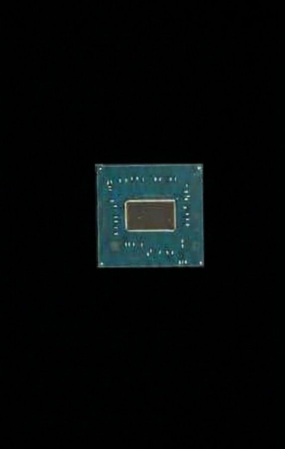
Also leaked in the last week by the same X (Twitter) user – a pic of Intel’s upcoming Z990 PCH. From VideoCardz:
The Z990 PCH package measures 25 x 24 mm. The exposed die reportedly measures 11.15 x 6.5 mm, which works out to around 72.5 mm². For comparison, Z890 measures 28 x 23.5 mm at package level and 11.376 x 8.165 mm at die level. This gives Z890 a package area of 658 mm² and a die area of around 92.9 mm². The reported Z990 package would be 600 mm², or around 8.8% smaller than Z890. The die would be around 22% smaller.
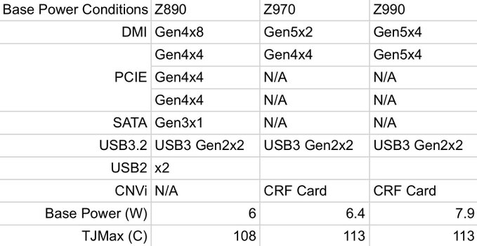
The leak states that Z990 could reach a peach power draw of 14 Watts, but only when fully loaded on it’s PCIe Gen 5.0 bus. More likely in our SFF world, it’ll draw around the 7-8 W, 1-2 Watts more than the current Z890 chipset. Also noted was Z970’s intended power draw of around 6.4W, closer to Z890 – likely due to increased the increased IO available. An increase of the rated TJMax has been implemented, moving up to 113 C, from the previous generation’s 108 C. For reference from the source:
Quite a few other leaks have come to light around the upcoming processor series, including mention that the top level SKU will be a 52 core (16P, 32E, 4LP), 150W base power behemoth, with likely a price tag to match. All I’m hoping for is more T series SKUs for us SFF folks!


